Labels

Showing posts with label Semiconductor physics. Show all posts

What is Vander pauw method for mobility measurement of semiconductors? Hall Voltage, quantized Hall Voltage?


Introduction: 

The Van der Pauw method is a technique for measuring the electrical resistivity and carrier mobility of a semiconductor material. The method was developed by L.J. van der Pauw in 1958 and is widely used in materials science and engineering.

The method involves measuring the electrical resistance of a sample using four probe contacts arranged in a square or rectangular configuration. The contacts are made on opposite sides of the sample, and the resistance is measured using a multimeter. The sample is then rotated by 90 degrees, and the resistance is measured again. By repeating these measurements for different configurations of the four-probe contacts, the electrical resistivity of the sample can be determined.

The Van der Pauw method can also be used to determine the carrier mobility of a semiconductor material. Carrier mobility is a measure of how easily charge carriers (electrons or holes) move through the material under the influence of an electric field. To measure the carrier mobility, the sample is subjected to a magnetic field perpendicular to the sample surface, and the electrical resistance is measured as before. By repeating the measurements for different magnetic field strengths and orientations, the carrier mobility can be calculated using the Hall effect equation.

Overall, the Van der Pauw method is a simple and accurate technique for measuring the electrical resistivity and carrier mobility of semiconductor materials. It is commonly used in research and industry for quality control and performance optimization of semiconductor devices. 


Top of Form

Hall effect measurement:

The Hall effect is a phenomenon in which a magnetic field applied perpendicular to a current-carrying conductor induces a voltage across the conductor in the direction perpendicular to both the magnetic field and the current. This effect was discovered by American physicist Edwin Hall in 1879.

Hall effect measurements are used to determine the electrical properties of materials, particularly their carrier concentration, mobility, and type (whether they are electrons or holes). In a Hall effect measurement, a sample of the material is placed in a magnetic field, and a current is passed through the sample in a direction perpendicular to both the magnetic field and the voltage that develops due to the Hall effect. By measuring the voltage across the sample and the current passing through it, the carrier concentration and mobility can be determined using the Hall effect equation.

The Hall effect measurement can provide valuable information about the electronic properties of materials, which is important in many applications such as semiconductor device design, material characterization, and quality control. For example, in semiconductor device design, the Hall effect measurement can be used to optimize the doping level and thickness of the semiconductor layers to achieve the desired electrical performance. In material characterization, the Hall effect measurement can be used to determine the effect of impurities and defects on the electrical properties of the material.


Sample preparation: 

Ohmic contacts are formed on the sample surface in a preferred way following ways figure 1:


Figure1: Van der Pauw method sample required

Overall, the Hall effect measurement is a powerful tool for understanding the electrical properties of materials and has many practical applications in industry and research.


Top of Form

What is Hall voltage and quantized Hall voltage?

The Hall voltage is the voltage that develops across a sample of a conducting material when a magnetic field is applied perpendicular to the flow of electrical current through the sample. The Hall voltage is proportional to the applied magnetic field, the current through the sample, and the carrier concentration and mobility of the charge carriers in the material. Figure 2 is the Hall measurement setup.


Figure 2: Hall voltage measurement principle

The Hall voltage is given by the Hall effect equation:

V_H = BIn*q / d

where V_H is the Hall voltage, B is the magnetic field strength, I is the current passing through the sample, n is the carrier concentration, q is the charge of the carriers, and d is the thickness of the sample.


The Van der Pauw configuration is shown in Figure 3.


Figure 3: Van dar Pauw configuration for Hall voltage measurement 


Quantized Hall voltage, also known as the integer quantum Halleffect (IQHE), is a phenomenon observed in two-dimensional electron systems in the presence of a strong magnetic field. In this regime, the Hall resistance (the ratio of Hall voltage to current) exhibits quantization at certain values, which are independent of the material properties and the geometry of the sample. The quantized Hall resistance is given by the equation:

R_H = (h/e^2) * (N + 1/2)

where R_H is the Hall resistance, h is Planck's constant, e is the elementary charge, and N is an integer known as the Landau level index. 


What is the landau level index?

In condensed matter physics, the Landau level index refers to a quantum number that characterizes the energy levels of electrons in a two-dimensional system subjected to a strong magnetic field perpendicular to the plane of the system. These energy levels are known as Landau levels, and the Landau level index is a measure of the quantized energy of electrons in a particular Landau level.

In a strong magnetic field, the electrons in a two-dimensional system occupy discrete energy levels, known as Landau levels, which are separated by a constant energy spacing known as cyclotron energy. The Landau level index, denoted by N, is an integer that specifies the energy level of an electron in the system, with higher values of N corresponding to higher energy levels. The energy of each Landau level is given by the equation:

E_N = (N + 1/2) * hbar * omega_c

where E_N is the energy of the Nth Landau level, hbar is the reduced Planck's constant, and omega_c is the cyclotron frequency, which is proportional to the applied magnetic field.

The Landau level index plays a crucial role in the phenomenon of the quantized Hall effect, where the Hall resistance of a two-dimensional system in a strong magnetic field exhibits quantization at certain values of the magnetic field strength and Landau level index. The quantization of the Hall resistance arises from the topological properties of the electron wave function in a magnetic field and is independent of the material properties and sample geometry.

The quantization of the Hall resistance is a result of the topological properties of the electron wave function in a magnetic field and has important implications for the study of condensed matter physics and the development of novel electronic devices.


Why do we need to measure quantized Hall voltage?

The quantized Hall voltage, also known as the integer quantum Hall effect (IQHE), is an important phenomenon to study in condensed matter physics because it provides a unique example of a topological quantum state of matter. The quantization of the Hall resistance in a two-dimensional electron gas in a strong magnetic field is independent of the sample geometry, impurities, and other perturbations, and is determined solely by fundamental constants such as Planck's constant and the elementary charge. This makes the IQHE an extremely precise standard for resistance measurement.

The quantized Hall voltage has several practical applications, especially in metrology, where it is used as a standard for the calibration of resistance measurement devices. The quantization of the Hall resistance is very precise, with a relative uncertainty of less than 10E-9, which makes it an ideal standard for resistance measurements in various fields such as materials science, electronics, and metrology.

Moreover, the IQHE has led to the discovery of many new phenomena in condensed matter physics, including the fractional quantum Hall effect, which is a phenomenon that occurs at lower magnetic fields and involves the quantization of the Hall resistance at fractional multiples of the standard quantized value. The study of these effects has led to the development of new theoretical models and insights into the behavior of electrons in condensed matter systems.

Overall, the measurement of quantized Hall voltage is important both for fundamental research and for practical applications, especially in metrology and resistance measurement. Find more diverse field discussions in the home page tabs here.
Why does HfO2 is better than SiO2 for electronic devices, specifically for MOSFET?

Introduction:

HfO2 is often preferred over SiO2 as a gate dielectric in MOSFETs (Metal-Oxide-Semiconductor Field-Effect Transistors) for several reasons:

  1. Higher dielectric constant: HfO2 has a higher dielectric constant than SiO2, which means that it can store more charge per unit area. This property allows for the creation of MOSFETs with higher capacitance, which can result in faster switching times and better performance.
  2. Better reliability: HfO2 has better reliability than SiO2, which is important for ensuring that MOSFETs have a long lifespan and are not susceptible to failure over time. HfO2 has a higher resistance to breakdown and thermal instability, which makes it more suitable for high-temperature applications.
  3. Compatibility with high-k metal gate electrodes: HfO2 is compatible with high-k metal gate electrodes, which are commonly used in MOSFETs. This compatibility allows for the creation of MOSFETs with better performance and reduced power consumption.
  4. Reduced gate leakage current: HfO2 has a lower gate leakage current than SiO2, which means that it is less susceptible to current leakage and can maintain a stable threshold voltage over time. This property is important for ensuring that MOSFETs are reliable and have consistent performance.

Overall, the properties of HfO2 make it a better choice than SiO2 for gate dielectrics in MOSFETs, as it can improve performance, reliability, and compatibility with other materials used in MOSFET fabrication.

Are their thickness being same for the device?

No, the thicknesses of HfO2 and SiO2 gate dielectrics are not typically the same in MOSFET devices. The thickness of the gate dielectric layer is an important parameter that can affect the performance and characteristics of the MOSFET.

Historically, SiO2 has been the most commonly used gate dielectric material in MOSFETs, with typical thicknesses ranging from a few nanometers to tens of nanometers. However, as device dimensions have continued to shrink, the use of SiO2 as a gate dielectric has become problematic due to increased leakage currents and reduced gate control.

HfO2, with its higher dielectric constant and better reliability, has emerged as a promising alternative to SiO2. Typical HfO2 thicknesses in MOSFET devices range from a few angstroms to a few nanometers, depending on the specific application and device requirements.

In general, the thickness of the gate dielectric layer is carefully optimized based on the specific requirements of the device, such as its operating voltage, power consumption, and switching speed. This optimization process takes into account factors such as gate leakage current, gate capacitance, and device reliability, among others.

Yes, HfO2 can be used as a ferroelectric gate material for ferroelectric FETs (Field-Effect Transistors). In fact, HfO2-based ferroelectric materials have been extensively studied for use as gate dielectrics in ferroelectric FETs.

Ferroelectric FETs are a type of transistor that use a ferroelectric material as the gate dielectric. Ferroelectric materials have the ability to switch polarization in response to an applied electric field, which makes them attractive for use in non-volatile memory devices and other applications.

HfO2-based ferroelectric materials have several advantages over other ferroelectric materials, such as Pb(Zr,Ti)O3 (PZT), including higher dielectric constant, better thermal stability, and compatibility with CMOS (Complementary Metal-Oxide-Semiconductor) technology. HfO2-based ferroelectric materials also have the potential for improved scalability and reduced processing complexity compared to other ferroelectric materials.

Several different types of HfO2-based ferroelectric materials have been developed, including doped HfO2, HfO2-ZrO2 alloys, and HfO2-TiO2 alloys. These materials have been shown to exhibit ferroelectric properties, such as hysteresis and polarization switching, and have been used to fabricate ferroelectric FETs with improved performance.

Overall, HfO2-based ferroelectric materials are a promising option for use as gate materials in ferroelectric FETs, and further research in this area is ongoing. Find more help here.

#3. What is HfO2 and it's properties? Physics properties

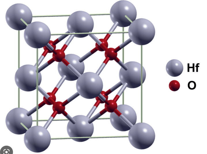
Introduction: Hafnium dioxide (HfO2) is a metal oxide compound that is commonly used in electronic devices as a high-k dielectric material. Its crystal structure of it is cubic (figure1).


Cubic phase HfO2. Hf is in FFC position 


Some of its key properties include:

  1. High dielectric constant: HfO2 has a high dielectric constant (k), which means that it can store a large amount of electric charge per unit area. This property is important for electronic devices because it allows for the creation of capacitors that can store more charge in a smaller area.
  2. Good thermal stability: HfO2 is stable at high temperatures, which makes it suitable for use in devices that operate at elevated temperatures.
  3. Good electrical properties: HfO2 has a high breakdown voltage and low leakage current, which are important for ensuring that electronic devices are reliable and have a long lifespan.
  4. High refractive index: HfO2 has a high refractive index, which makes it useful for creating optical coatings and thin films for applications such as solar cells and LEDs.
  5. Compatibility with silicon technology: HfO2 is compatible with silicon technology, which makes it easy to integrate into existing electronic devices.

What are the physical properties of HfO2?

Hafnium oxide (HfO2) is a chemical compound that has several physical properties, including:

Density: HfO2 has a density of approximately 9.68 g/cm³ at room temperature.

 Melting point: The melting point of HfO2 is very high, around 2,760°C or 4,999°F.

Hardness: HfO2 is a very hard material, with a Mohs hardness of approximately 7.5.

Refractive index: The refractive index of HfO2 is around 2.1, which means that it has a relatively high level of optical clarity.

Thermal conductivity: HfO2 has a high thermal conductivity, which means that it can conduct heat very effectively.

Electrical conductivity: HfO2 is an insulator, meaning it does not conduct electricity well.

Color: HfO2 is typically white or off-white in color.

Solubility: HfO2 is not soluble in water or organic solvents.

Dielectric properties of HfO2?

Hafnium oxide (HfO2) is a high-k dielectric material, which means it has a high relative permittivity or dielectric constant (εr). Here are some dielectric properties of HfO2:

  1. Dielectric constant: HfO2 has a high dielectric constant ranging from 20 to 25, which is significantly higher than that of conventional SiO2 dielectrics.
  2. Dielectric loss: HfO2 has low dielectric loss, which makes it suitable for use in high-frequency applications.
  3. Breakdown strength: HfO2 has a high breakdown strength, which makes it resistant to electrical breakdown under high voltage stress.
  4. Leakage current: HfO2 has low leakage current density, which means that it can store charge for longer periods of time.

These dielectric properties make HfO2 an attractive material for use as a gate dielectric in metal-oxide-semiconductor field-effect transistors (MOSFETs) and as a dielectric in capacitors. HfO2-based dielectrics have enabled further miniaturization of electronic devices and improved their performance.

These physical and dielectric properties make HfO2 a useful material in various applications, including as a high-temperature electrical insulator, as a thermal barrier coating, and in the production of optical coatings and components. Overall, HfO2 is a versatile material with a range of useful properties that make it well-suited for use in electronic devices and other applications find more help here.

#2. How do electrode defects affects it's I-V properties?

Introduction:

Electrode defects can have a significant impact on the I-V properties (current-voltage characteristics) of an electrode. The specific effects of electrode defects on I-V properties depend on the type and severity of the defect. Some possible effects of electrode defects on I-V properties include:

  1. Increased resistance: If the electrode has defects that increase its resistance, the I-V curve will show a decrease in current for a given voltage. This is because the current flow through the electrode is hindered by the increased resistance.
  2. Non-ohmic behavior: In ideal conditions, the I-V curve of an electrode should be linear, following Ohm's Law. However, electrode defects can cause deviations from this linear behavior, resulting in non-ohmic I-V curves. For example, a defect may cause the electrode to exhibit rectifying behavior, meaning that the current flow is significantly higher in one direction than the other.
  3. Shifted or distorted I-V curve: Depending on the type and location of the defect, the I-V curve may shift or become distorted. This can make it difficult to accurately measure or predict the electrode's performance.
  4. Reduced stability: Electrode defects can also reduce the stability of the electrode, causing changes in its I-V properties over time. This can be especially problematic in applications where the electrode is frequently used or exposed to harsh conditions.

Overall, electrode defects can significantly impact an electrode's I-V properties, which can affect its performance in various applications. It is therefore important to carefully monitor and control for electrode defects in order to ensure optimal performance. An example of the electrode size-dependent elsewhere. A typical electrode size-dependent I-V behavior is shown in Figure 1. 

Figure1: Electrode size dependent-I-V response(example)


 Does a defective surface have a different vertical I-V response if the electrode is good?

Yes, a defective surface can have a different vertical I-V response compared to a non-defective surface, even if the electrode is good. This is because defects on the surface of a material can affect its electronic properties, such as its conductivity, charge transport, and carrier lifetime. These changes can lead to variations in the electrical response of the material, including its I-V properties.

For example, if a surface defect creates a local trap state that captures and traps charge carriers, it can reduce the measured current in the vertical I-V response. Alternatively, if the defect creates a non-uniform electric field that alters the local carrier mobility or density, it can result in changes to the slope or shape of the I-V curve.

In general, defects on the surface of a material can have complex and varied effects on its electrical response, and the specific nature of these effects will depend on the type and location of the defect, as well as the properties of the surrounding material and electrode. Therefore, it is important to carefully characterize and control for surface defects in order to accurately interpret and understand the electrical response of a material. find more help here. 

#1# What is materials science and technology? Roles of scientist and engineer.

 #1# What is materials science and technology? Roles of scientist and engineer.

Introduction: Materials Science and Technology (MST) is a field of study that investigates the properties and behavior of various materials, such as metals, polymers, ceramics, and composites. It is an interdisciplinary field that combines elements of physics, chemistry, engineering and applied mathematics to understand the relationships between the structure, properties, processing, and performance of materials (figure 1).Figure.1. Materials science connections

Figure.1. Materials science connections


Materials scientists and technologists seek to develop new materials with unique properties and improve existing materials. They investigate the structure of materials at various scales, from the atomic and molecular level to the macroscopic level, and use this knowledge to design materials with desired properties. They also study how materials respond to different conditions, such as temperature, pressure, and stress.

Materials science and technology have a wide range of applications, including aerospace and transportation, electronics, energy, biomedical engineering, and nanotechnology. It plays a critical role in the development of new technologies and products and in the advancement of industries that rely on materials.

What are the major roles of materials scientists and engineers?

Materials scientists and engineers play a critical role in developing and improving materials that are used in various industries. Here are some of the major roles they play:

  1. Research and development: Materials scientists and engineers conduct research to develop new materials with desired properties or improve existing materials. They work on materials at the atomic and molecular level and use techniques such as X-ray diffraction, microscopy, and spectroscopy to study their structure, properties, and behavior.
  2. Material selection: Materials scientists and engineers select the appropriate materials for a particular application based on their properties, cost, availability, and environmental impact. They consider factors such as strength, durability, corrosion resistance, thermal and electrical conductivity, and toxicity.
  3. Testing and characterization: Materials scientists and engineers test and characterize materials to determine their properties, such as strength, hardness, elasticity, and ductility. They use various techniques like mechanical testing, thermal analysis, and spectroscopy.
  4. Process development: Materials scientists and engineers develop and optimize processes for producing materials with desired properties. They consider factors such as temperature, pressure, composition, and time to control the structure and properties of the materials.
  5. Quality control: Materials scientists and engineers ensure that materials meet the required standards and specifications for their intended use. They develop and implement quality control procedures to ensure the consistency and reliability of the materials.
  6. Problem-solving: Materials scientists and engineers solve problems related to materials'      performance and failure. They use their knowledge of materials' properties and behavior to identify the root causes of the problems and develop solutions to prevent them from recurring.
Figure2: Laboratory activities to make something new for science and technology

Overall, materials scientists and engineers play a critical role in advancing technology and improving the quality of life by developing and improving the materials that are used in various industries. More about science and technology help.

Low power and high power semiconductor devices and major application area.

 Introduction:

Low power and high power semiconductor devices are categorized based on their ability to handle power and current levels. Here are some of the major low power and high power semiconductor devices:

Low Power Semiconductor Devices:
Bipolar Junction Transistors (BJTs)
Junction Field-Effect Transistors (JFETs)
Small Signal Diodes
Zener Diodes
Schottky Diodes
High Power Semiconductor Devices:
Insulated Gate Bipolar Transistors (IGBTs)
Power Metal-Oxide-Semiconductor Field-Effect Transistors (MOSFETs)
Thyristors (Silicon Controlled Rectifiers (SCRs), Triacs)
Power Diodes
Gallium Nitride (GaN) Devices
Silicon Carbide (SiC) Devices

Low power:


Low power semiconductor devices are typically used in applications where small currents and voltages are involved, such as in signal processing and low-power electronics. These devices have low power dissipation, low voltage drop, and high input impedance, making them suitable for low power applications.

High power: 

High power semiconductor devices, on the other hand, are used in applications where high current and voltage levels are required, such as in power electronics, electric vehicles, and renewable energy systems. These devices have high power dissipation, high voltage blocking capability, and low on-state resistance, making them suitable for high power applications.

Overall, the choice of low power or high power semiconductor devices depends on the specific application requirements, such as power level, voltage level, and switching frequency.


Applications:

Semiconductor devices have a wide range of applications in various fields, including electronics, telecommunications, computing, energy, and transportation. Here are some of the major application areas of semiconductor devices:

Electronics: Semiconductors are the foundation of modern electronics, and they are used in a wide range of devices, such as smartphones, computers, televisions, and gaming consoles. They are also used in sensors, amplifiers, oscillators, and memory devices.

Telecommunications: Semiconductors are used in telecommunications equipment, such as cell phones, base stations, and routers. They are also used in fiber optic cables, satellite communication systems, and microwave devices.

Computing: Semiconductors are essential components in computing devices, such as processors, memory chips, and storage devices. They are also used in graphics cards, sound cards, and other peripheral devices.

Energy: Semiconductors play a critical role in renewable energy systems, such as solar panels and wind turbines. They are also used in power electronics, such as inverters, rectifiers, and DC-DC converters.

Transportation: Semiconductors are used in various transportation systems, such as electric vehicles, hybrid vehicles, and aircraft. They are also used in control systems for engines, brakes, and suspension systems.

Overall, semiconductor devices have revolutionized many aspects of modern life, and their applications are constantly expanding as new technologies and innovations emerge. Please find more here.

What is green energy mission(GEM)? Key area of GEM? Si, GaN, SiC, GaAs, special Ga2O3

 Introduction: 


The Green Energy Mission in semiconductor research field focuses on developing energy-efficient technologies and processes to reduce the environmental impact of semiconductor manufacturing and promote sustainable energy solutions. Semiconductor manufacturing is an energy-intensive process that requires a significant amount of electricity and produces greenhouse gases and other pollutants. The Green Energy Mission seeks to address these environmental concerns by developing new technologies and processes that reduce energy consumption and carbon emissions.


Key Green areas: 

Some of the key areas of research in the Green Energy Mission include:

Energy-efficient semiconductor manufacturing: Researchers are developing new techniques to reduce energy consumption and carbon emissions in semiconductor manufacturing, such as using renewable energy sources, optimizing manufacturing processes, and developing energy-efficient devices.

Renewable energy: Semiconductors play a critical role in renewable energy systems, such as solar panels and wind turbines. Researchers are working to improve the efficiency and reduce the cost of these systems to promote widespread adoption.

Energy storage: Semiconductor devices are used in energy storage systems, such as batteries and capacitors. Researchers are developing new materials and processes to improve the performance and reduce the environmental impact of these systems.

Energy harvesting: Researchers are developing semiconductor-based technologies to harvest energy from renewable sources, such as solar and kinetic energy, to power small devices and sensors.

Overall, the Green Energy Mission in semiconductor research aims to develop sustainable and energy-efficient technologies that promote environmental sustainability and reduce the dependence on fossil fuels.

Yes, here is a list of some of the commonly used power semiconductor materials:


Semiconductor materials:


Silicon (Si): Silicon is the most widely used material for power semiconductor devices due to its abundance, low cost, and excellent electrical properties. It is used in devices such as diodes, thyristors, and insulated gate bipolar transistors (IGBTs).

Gallium nitride (GaN): GaN is a wide bandgap semiconductor material that offers superior performance compared to silicon in terms of efficiency, switching speed, and power density. It is used in devices such as power transistors, diodes, and rectifiers for high-frequency and high-power applications.

Silicon carbide (SiC): SiC is another wide bandgap semiconductor material that offers superior performance compared to silicon, especially at high temperatures and high voltages. It is used in devices such as Schottky diodes, MOSFETs, and thyristors for high-power and high-temperature applications.

Diamond: Diamond is an emerging power semiconductor material that offers the highest thermal conductivity, allowing for better heat dissipation and higher power density. It is still in the research and development stage, but has the potential to revolutionize power electronics technology.

Gallium arsenide (GaAs): GaAs is a high-performance semiconductor material that offers superior electron mobility and high-frequency performance. It is used in devices such as microwave transistors, amplifiers, and switches for telecommunications and defense applications.

Overall, power semiconductor materials play a critical role in the development of power electronics technology, and each material has its unique advantages and limitations depending on the application requirements. 

However, Gallium Oxide (Ga2O3) is another emerging wide bandgap semiconductor material that has shown promise for high-power and high-voltage applications. Ga2O3 has a much wider bandgap than silicon, GaN, and SiC, making it suitable for use in power devices that require high breakdown voltage, high current density, and low on-resistance. Importance of power semiconductor device for green energy can be easily understand from here. Fig 1 shows a brief relation of 


Some of the potential feasibility and concerns of Ga2O3 as a power semiconductor.


High breakdown voltage: Ga2O3 has a high critical field strength, which allows it to withstand higher voltages without breakdown.

High current density: Ga2O3 has a high electron mobility, which allows it to carry more current than other wide bandgap materials.

Low on-resistance: Ga2O3 has a low specific on-resistance, which means that it can operate at lower voltages and consume less power.

Low cost: Ga2O3 is abundant and relatively low-cost compared to other wide bandgap materials.

Some of the potential applications of Ga2O3 power devices include high-voltage power supplies, electric vehicles, renewable energy systems, and high-power electronics for aerospace and defense.

Although Ga2O3 is still in the early stages of development, researchers are working on improving the quality of the material and developing new device structures to harness its full potential as a power semiconductor material. like any emerging semiconductor material, Gallium Oxide (Ga2O3) has some drawbacks that need to be addressed before it can be widely adopted in power electronics applications. Some of the major drawbacks of Ga2O3 include:

Crystal quality: Ga2O3 is a relatively new material, and its crystal quality is not yet as good as other wide bandgap materials such as SiC and GaN. Poor crystal quality can lead to defects and reduced performance in power devices.

Fabrication challenges: Ga2O3 is a complex material to fabricate into power devices, and the existing processes are not as mature as those for SiC and GaN. Developing reliable and scalable fabrication processes will be critical to the commercialization of Ga2O3 power devices.

Thermal conductivity: While Ga2O3 has a high breakdown voltage and low on-resistance, its thermal conductivity is lower than that of other wide bandgap materials. This can lead to higher operating temperatures and thermal management challenges in power devices.

Limited availability: While Ga2O3 is abundant, the supply of high-quality material for power electronics applications is limited. Developing cost-effective and scalable methods for producing high-quality Ga2O3 will be important for its widespread adoption.

Overall, while Ga2O3 has many potential advantages as a power semiconductor material, there are still several technical challenges that need to be overcome before it can be widely adopted in power electronics applications. Researchers are actively working on addressing these challenges to unlock the full potential of Ga2O3 as a power semiconductor material. Please find more information here.