Introduction:
Gallium oxide (Ga2O3) is a complex material with many possible defects that can arise during its growth and processing. The basic crystal structure of Ga2O3 is shown in figure 1 of most stable beta-phase.
Figure 1: Beta phase crystal structure of Ga2O3

Some of the most common defects in Ga2O3 include:
Defects in Ga2O3:
Oxygen vacancies: Oxygen vacancies are defects in which an oxygen atom is missing from the crystal lattice. These defects can create localized states in the bandgap, leading to changes in the electrical and optical properties of the material.
Gallium vacancies: Gallium vacancies are defects in which a gallium atom is missing from the crystal lattice. These defects can also create localized states in the bandgap and affect the electronic properties of the material.
Point defects: Point defects are localized disruptions in the crystal lattice, such as interstitial atoms or impurities. These defects can alter the electrical and optical properties of the material, as well as affect its mechanical and thermal properties.
Dislocations: Dislocations are line defects in the crystal lattice that can arise during crystal growth or processing. These defects can affect the mechanical and electrical properties of the material and reduce its performance in power devices.
Grain boundaries: Grain boundaries are interfaces between different crystal grains in the material. These interfaces can create defects and alter the electrical and mechanical properties of the material.
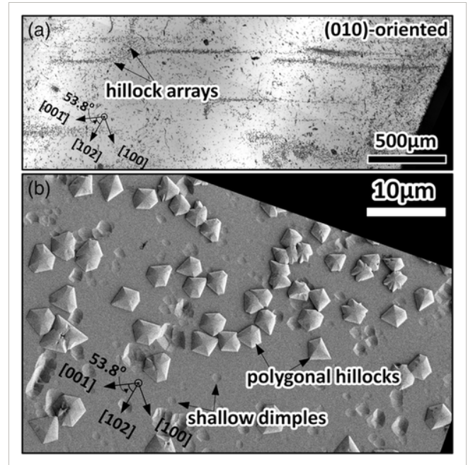
An example of dislocation is shown in figure 2.
Overall, understanding and controlling the defects in Ga2O3 is critical for developing high-quality material for power electronics applications. Researchers are actively working on characterizing and controlling these defects to improve the performance and reliability of Ga2O3 power devices.
P-type Ga2O3:
Although it is more difficult than making n-type Ga2O3. The challenge in making p-type Ga2O3 is that the native defects in the material tend to be n-type, which makes it difficult to introduce p-type dopants such as magnesium (Mg) or zinc (Zn).
One approach to making p-type Ga2O3 is to introduce acceptor dopants such as Mg or Zn into the material and then anneal the sample under oxygen-deficient conditions. This can create oxygen vacancies in the material, which can then capture electrons and create holes, resulting in p-type behavior.
Another approach is to use co-doping, in which both an acceptor dopant (e.g., Mg) and a compensating donor dopant (e.g., Si) are introduced into the material. The donor dopant can introduce electrons into the material to compensate for the holes created by the acceptor dopant, resulting in p-type behavior.
While p-type Ga2O3 has been demonstrated in the laboratory, it is still challenging to achieve high-quality p-type material with good stability and reproducibility. Further research is needed to develop reliable and scalable methods for making p-type Ga2O3 and integrating it into power devices.
Nitrogen doping has also been explored as a potential method for achieving p-type conductivity in Ga2O3. Nitrogen is an acceptor dopant, which means it can introduce holes in the material when it substitutes for oxygen in the crystal lattice.
Several studies have reported successful nitrogen doping in Ga2O3, resulting in p-type behavior. For example, one study reported that nitrogen doping using plasma-assisted molecular beam epitaxy (MBE) could achieve p-type conductivity in Ga2O3 with a hole concentration of up to 10^17 cm^-3 and a hole mobility of 3 cm^2/Vs. Another study reported that nitrogen doping using ion implantation and annealing could achieve p-type conductivity with a hole concentration of up to 10^18 cm^-3.
However, the stability and reproducibility of nitrogen-doped Ga2O3 have not been well-established, and more research is needed to develop reliable and scalable methods for nitrogen doping in Ga2O3. Additionally, the use of nitrogen as a dopant in Ga2O3 can introduce defects and alter the material's properties, so careful optimization of the doping process is needed to minimize these effects. More discussion of semiconductor is here for green device concepts and basic about semiconductor devices.
No comments:
Post a Comment