Low power and high power semiconductor devices and major application area.

 Introduction:

Low power and high power semiconductor devices are categorized based on their ability to handle power and current levels. Here are some of the major low power and high power semiconductor devices:

Low Power Semiconductor Devices:
Bipolar Junction Transistors (BJTs)
Junction Field-Effect Transistors (JFETs)
Small Signal Diodes
Zener Diodes
Schottky Diodes
High Power Semiconductor Devices:
Insulated Gate Bipolar Transistors (IGBTs)
Power Metal-Oxide-Semiconductor Field-Effect Transistors (MOSFETs)
Thyristors (Silicon Controlled Rectifiers (SCRs), Triacs)
Power Diodes
Gallium Nitride (GaN) Devices
Silicon Carbide (SiC) Devices

Low power:


Low power semiconductor devices are typically used in applications where small currents and voltages are involved, such as in signal processing and low-power electronics. These devices have low power dissipation, low voltage drop, and high input impedance, making them suitable for low power applications.

High power: 

High power semiconductor devices, on the other hand, are used in applications where high current and voltage levels are required, such as in power electronics, electric vehicles, and renewable energy systems. These devices have high power dissipation, high voltage blocking capability, and low on-state resistance, making them suitable for high power applications.

Overall, the choice of low power or high power semiconductor devices depends on the specific application requirements, such as power level, voltage level, and switching frequency.


Applications:

Semiconductor devices have a wide range of applications in various fields, including electronics, telecommunications, computing, energy, and transportation. Here are some of the major application areas of semiconductor devices:

Electronics: Semiconductors are the foundation of modern electronics, and they are used in a wide range of devices, such as smartphones, computers, televisions, and gaming consoles. They are also used in sensors, amplifiers, oscillators, and memory devices.

Telecommunications: Semiconductors are used in telecommunications equipment, such as cell phones, base stations, and routers. They are also used in fiber optic cables, satellite communication systems, and microwave devices.

Computing: Semiconductors are essential components in computing devices, such as processors, memory chips, and storage devices. They are also used in graphics cards, sound cards, and other peripheral devices.

Energy: Semiconductors play a critical role in renewable energy systems, such as solar panels and wind turbines. They are also used in power electronics, such as inverters, rectifiers, and DC-DC converters.

Transportation: Semiconductors are used in various transportation systems, such as electric vehicles, hybrid vehicles, and aircraft. They are also used in control systems for engines, brakes, and suspension systems.

Overall, semiconductor devices have revolutionized many aspects of modern life, and their applications are constantly expanding as new technologies and innovations emerge. Please find more here.

What is green energy mission(GEM)? Key area of GEM? Si, GaN, SiC, GaAs, special Ga2O3

 Introduction: 


The Green Energy Mission in semiconductor research field focuses on developing energy-efficient technologies and processes to reduce the environmental impact of semiconductor manufacturing and promote sustainable energy solutions. Semiconductor manufacturing is an energy-intensive process that requires a significant amount of electricity and produces greenhouse gases and other pollutants. The Green Energy Mission seeks to address these environmental concerns by developing new technologies and processes that reduce energy consumption and carbon emissions.


Key Green areas: 

Some of the key areas of research in the Green Energy Mission include:

Energy-efficient semiconductor manufacturing: Researchers are developing new techniques to reduce energy consumption and carbon emissions in semiconductor manufacturing, such as using renewable energy sources, optimizing manufacturing processes, and developing energy-efficient devices.

Renewable energy: Semiconductors play a critical role in renewable energy systems, such as solar panels and wind turbines. Researchers are working to improve the efficiency and reduce the cost of these systems to promote widespread adoption.

Energy storage: Semiconductor devices are used in energy storage systems, such as batteries and capacitors. Researchers are developing new materials and processes to improve the performance and reduce the environmental impact of these systems.

Energy harvesting: Researchers are developing semiconductor-based technologies to harvest energy from renewable sources, such as solar and kinetic energy, to power small devices and sensors.

Overall, the Green Energy Mission in semiconductor research aims to develop sustainable and energy-efficient technologies that promote environmental sustainability and reduce the dependence on fossil fuels.

Yes, here is a list of some of the commonly used power semiconductor materials:


Semiconductor materials:


Silicon (Si): Silicon is the most widely used material for power semiconductor devices due to its abundance, low cost, and excellent electrical properties. It is used in devices such as diodes, thyristors, and insulated gate bipolar transistors (IGBTs).

Gallium nitride (GaN): GaN is a wide bandgap semiconductor material that offers superior performance compared to silicon in terms of efficiency, switching speed, and power density. It is used in devices such as power transistors, diodes, and rectifiers for high-frequency and high-power applications.

Silicon carbide (SiC): SiC is another wide bandgap semiconductor material that offers superior performance compared to silicon, especially at high temperatures and high voltages. It is used in devices such as Schottky diodes, MOSFETs, and thyristors for high-power and high-temperature applications.

Diamond: Diamond is an emerging power semiconductor material that offers the highest thermal conductivity, allowing for better heat dissipation and higher power density. It is still in the research and development stage, but has the potential to revolutionize power electronics technology.

Gallium arsenide (GaAs): GaAs is a high-performance semiconductor material that offers superior electron mobility and high-frequency performance. It is used in devices such as microwave transistors, amplifiers, and switches for telecommunications and defense applications.

Overall, power semiconductor materials play a critical role in the development of power electronics technology, and each material has its unique advantages and limitations depending on the application requirements. 

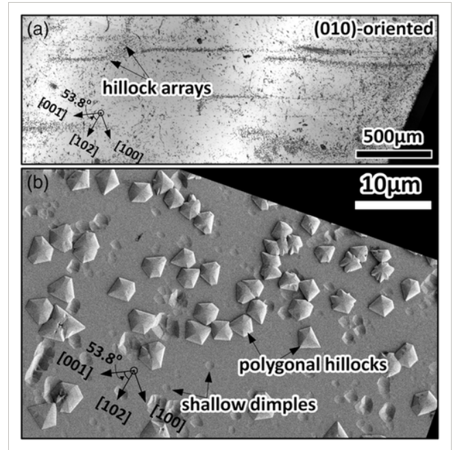
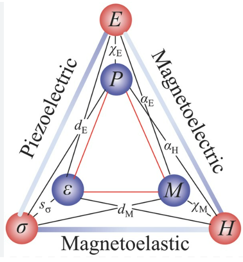
However, Gallium Oxide (Ga2O3) is another emerging wide bandgap semiconductor material that has shown promise for high-power and high-voltage applications. Ga2O3 has a much wider bandgap than silicon, GaN, and SiC, making it suitable for use in power devices that require high breakdown voltage, high current density, and low on-resistance. Importance of power semiconductor device for green energy can be easily understand from here. Fig 1 shows a brief relation of 


Some of the potential feasibility and concerns of Ga2O3 as a power semiconductor.


High breakdown voltage: Ga2O3 has a high critical field strength, which allows it to withstand higher voltages without breakdown.

High current density: Ga2O3 has a high electron mobility, which allows it to carry more current than other wide bandgap materials.

Low on-resistance: Ga2O3 has a low specific on-resistance, which means that it can operate at lower voltages and consume less power.

Low cost: Ga2O3 is abundant and relatively low-cost compared to other wide bandgap materials.

Some of the potential applications of Ga2O3 power devices include high-voltage power supplies, electric vehicles, renewable energy systems, and high-power electronics for aerospace and defense.

Although Ga2O3 is still in the early stages of development, researchers are working on improving the quality of the material and developing new device structures to harness its full potential as a power semiconductor material. like any emerging semiconductor material, Gallium Oxide (Ga2O3) has some drawbacks that need to be addressed before it can be widely adopted in power electronics applications. Some of the major drawbacks of Ga2O3 include:

Crystal quality: Ga2O3 is a relatively new material, and its crystal quality is not yet as good as other wide bandgap materials such as SiC and GaN. Poor crystal quality can lead to defects and reduced performance in power devices.

Fabrication challenges: Ga2O3 is a complex material to fabricate into power devices, and the existing processes are not as mature as those for SiC and GaN. Developing reliable and scalable fabrication processes will be critical to the commercialization of Ga2O3 power devices.

Thermal conductivity: While Ga2O3 has a high breakdown voltage and low on-resistance, its thermal conductivity is lower than that of other wide bandgap materials. This can lead to higher operating temperatures and thermal management challenges in power devices.

Limited availability: While Ga2O3 is abundant, the supply of high-quality material for power electronics applications is limited. Developing cost-effective and scalable methods for producing high-quality Ga2O3 will be important for its widespread adoption.

Overall, while Ga2O3 has many potential advantages as a power semiconductor material, there are still several technical challenges that need to be overcome before it can be widely adopted in power electronics applications. Researchers are actively working on addressing these challenges to unlock the full potential of Ga2O3 as a power semiconductor material. Please find more information here.


Defects and feasibility of p-Ga2O3 potentials and challenges for Green energy mission.

Introduction:

Gallium oxide (Ga2O3) is a complex material with many possible defects that can arise during its growth and processing. The basic crystal structure of Ga2O3 is shown in figure 1 of most stable beta-phase


Figure 1: Beta phase crystal structure of Ga2O3


Some of the most common defects in Ga2O3 include:

Defects in Ga2O3:

Oxygen vacancies: Oxygen vacancies are defects in which an oxygen atom is missing from the crystal lattice. These defects can create localized states in the bandgap, leading to changes in the electrical and optical properties of the material.

Gallium vacancies: Gallium vacancies are defects in which a gallium atom is missing from the crystal lattice. These defects can also create localized states in the bandgap and affect the electronic properties of the material.

Point defects: Point defects are localized disruptions in the crystal lattice, such as interstitial atoms or impurities. These defects can alter the electrical and optical properties of the material, as well as affect its mechanical and thermal properties.

Dislocations: Dislocations are line defects in the crystal lattice that can arise during crystal growth or processing. These defects can affect the mechanical and electrical properties of the material and reduce its performance in power devices.

Grain boundaries: Grain boundaries are interfaces between different crystal grains in the material. These interfaces can create defects and alter the electrical and mechanical properties of the material. 

An example of dislocation is shown in figure 2.

Overall, understanding and controlling the defects in Ga2O3 is critical for developing high-quality material for power electronics applications. Researchers are actively working on characterizing and controlling these defects to improve the performance and reliability of Ga2O3 power devices.

P-type Ga2O3:

Although it is more difficult than making n-type Ga2O3. The challenge in making p-type Ga2O3 is that the native defects in the material tend to be n-type, which makes it difficult to introduce p-type dopants such as magnesium (Mg) or zinc (Zn).

One approach to making p-type Ga2O3 is to introduce acceptor dopants such as Mg or Zn into the material and then anneal the sample under oxygen-deficient conditions. This can create oxygen vacancies in the material, which can then capture electrons and create holes, resulting in p-type behavior.

Another approach is to use co-doping, in which both an acceptor dopant (e.g., Mg) and a compensating donor dopant (e.g., Si) are introduced into the material. The donor dopant can introduce electrons into the material to compensate for the holes created by the acceptor dopant, resulting in p-type behavior.

While p-type Ga2O3 has been demonstrated in the laboratory, it is still challenging to achieve high-quality p-type material with good stability and reproducibility. Further research is needed to develop reliable and scalable methods for making p-type Ga2O3 and integrating it into power devices.

Nitrogen doping has also been explored as a potential method for achieving p-type conductivity in Ga2O3. Nitrogen is an acceptor dopant, which means it can introduce holes in the material when it substitutes for oxygen in the crystal lattice.

Several studies have reported successful nitrogen doping in Ga2O3, resulting in p-type behavior. For example, one study reported that nitrogen doping using plasma-assisted molecular beam epitaxy (MBE) could achieve p-type conductivity in Ga2O3 with a hole concentration of up to 10^17 cm^-3 and a hole mobility of 3 cm^2/Vs. Another study reported that nitrogen doping using ion implantation and annealing could achieve p-type conductivity with a hole concentration of up to 10^18 cm^-3.

However, the stability and reproducibility of nitrogen-doped Ga2O3 have not been well-established, and more research is needed to develop reliable and scalable methods for nitrogen doping in Ga2O3. Additionally, the use of nitrogen as a dopant in Ga2O3 can introduce defects and alter the material's properties, so careful optimization of the doping process is needed to minimize these effects. More discussion of semiconductor is here for green device concepts and basic about semiconductor devices.

What is multi-ferroic?Device target, Major challenges.

 Introduction:

What is multi-ferroelectric material?

A multi-ferroic material is a type of material that exhibits multiple types of ferroic ordering, such as ferromagnetism, ferroelectricity, and ferro-elasticity, in a single material. In other words, these materials can have more than one ferroic property simultaneously.

Ferroic materials are characterized by the existence of a spontaneous polarization or magnetization, which can be switched or reversed by an applied electric or magnetic field, respectively. Ferromagnetic materials, for example, exhibit a spontaneous magnetization, while ferroelectric materials exhibit a spontaneous electric polarization. Ferroelastic materials exhibit a spontaneous deformation or strain.

Multi-ferroic materials are of great interest because they offer the potential for new types of functional materials and devices, such as magnetoelectric sensors, actuators, and memory devices. For example, a magnetoelectric memory device could store data as both magnetic and electric signals, which could provide enhanced performance and energy efficiency compared to traditional memory technologies. How they are connected each other is shown in figure 1.

Some examples of multi-ferroic materials include bismuth ferrite (BiFeO3), which exhibits both ferroelectric and antiferromagnetic orderings, and lead magnesium niobate-lead titanate (PMN-PT), which exhibits both ferroelectric and ferroelastic orderings. Research is ongoing to explore new types of multi-ferroic materials and to understand the underlying physics that govern their behavior.

Ferroic in one materials?


materials can have both ferromagnetic and ferroelectric characteristics, and such materials are called "magnetoelectric multiferroics." These materials exhibit both magnetic and electric polarizations that are coupled to each other, allowing for control of one property with the other. The coupling between magnetic and electric polarizations in these materials can be exploited for various applications, including magnetoelectric sensors, actuators, and memory devices.

One example of a magnetoelectric multiferroic material is bismuth ferrite (BiFeO3), which exhibits both ferroelectric and antiferromagnetic orderings. Another example is TbMnO3, which exhibits ferromagnetism and ferroelectricity at low temperatures.

Magnetoelectric multiferroics are still an area of active research, and many challenges remain in developing practical devices based on these materials. One challenge is to optimize the coupling between the magnetic and electric polarizations, as this coupling can be weak in some materials. Another challenge is to develop methods for integrating these materials into practical devices with high performance and reliability. However, the potential applications of magnetoelectric multiferroics make them an exciting area of research with significant potential for technological innovation.

Device target and concepts:


Multi-ferroic materials are materials that exhibit both ferromagnetic and ferroelectric properties simultaneously. In other words, these materials possess magnetic and electric ordering that can be controlled by each other. The device concept of multi-ferroic materials involves the development of devices that exploit the unique properties of these materials for various applications.

One such application is in data storage devices, where multi-ferroic materials can be used to develop non-volatile memories. The electric field can be used to control the magnetic state of the material, leading to the possibility of developing magnetic random access memory (MRAM) devices with low power consumption and high speed and vice versa. Figure 2 shows a conceptual device with multiferroic concept. 

Another potential application is in sensors and actuators. Multi-ferroic materials can be used to develop sensors that can detect both magnetic and electric fields simultaneously, which can have applications in medical imaging and non-destructive testing. Additionally, multi-ferroic materials can also be used to develop actuators that can be controlled using either magnetic or electric fields, which can be useful in the development of microelectromechanical systems (MEMS).

Overall, the device concept of multi-ferroic materials has significant potential for various applications, including data storage, sensing, and actuation, and ongoing research in this area is expected to lead to the development of new and innovative devices.

Major challenges:


There are several major challenges associated with magnetoelectric multiferroic materials that are currently being addressed by researchers in the field. Some of these challenges include:

Finding new materials: Currently, there are only a limited number of materials that exhibit both ferromagnetic and ferroelectric properties, and most of these materials have low magnetoelectric coupling. Thus, one major challenge is to find new materials that exhibit strong magnetoelectric coupling and are suitable for practical applications.

Understanding the underlying physics: The physics of magnetoelectric coupling is still not well understood, and more research is needed to understand the mechanisms that govern the coupling between magnetic and electric properties.

Developing practical devices: Magnetoelectric multiferroic materials have the potential to enable new types of devices, such as magnetoelectric sensors, actuators, and memory devices. However, there are still significant challenges associated with developing practical devices based on these materials, such as achieving high sensitivity, reliability, and manufacturability.

Controlling domain structure: The domain structure of magnetoelectric multiferroic materials can have a significant impact on their properties and performance. However, controlling the domain structure of these materials is a significant challenge, and more research is needed to develop effective methods for controlling domain structure at the nanoscale.

Temperature effect: Temperature can have a significant effect on the properties of magnetoelectric multiferroic materials. The ferromagnetic and ferroelectric properties of these materials are often strongly coupled, and changes

Overall, magnetoelectric multiferroic materials are a promising area of research, but there are still many challenges that must be addressed before they can be effectively integrated into practical devices. Please find other fruitful discussion here.